Abstract
We report field-plated Schottky rectifiers of various dimensions (circular geometry with diameter 50–200 μm and square diodes with areas 4 × 10⁻³–10−2 cm2) fabricated on thick (20μm), lightly doped (n = 2.10 × 1015 cm −3) β-Ga2O3 epitaxial layers grown by Hydride Vapor Phase Epitaxy on conducting (n = 3.6 × 1018 cm−3) substrates grown by Edge-Defined, Film-Fed growth. The maximum reverse breakdown voltage (VB) was 2300V for a 150 μm diameter device (area = 1.77 × 10⁻⁴ cm−2), corresponding to a breakdown field of 1.15 MV.cm−1. The reverse current was only 15.6 μA at this voltage. This breakdown voltage is highest reported for Ga2O3 rectifiers. The on-state resistance (RON) for these devices was 0.25 Ω.cm2, leading to a figure of merit (VB2/RON) of 21.2 MW.cm−2. The Schottky barrier height of the Ni was 1.03 eV, with an ideality factor of 1.1 and a Richardson's constant of 43.35 A.cm−2.K−2 obtained from the temperature dependence of the forward current density. The breakdown voltages for the different size devices ranged from 1400–2300V, with a general, but not linear trend of decreasing breakdown voltage for larger area rectifiers. The reverse recovery time was ∼22 ns for switching from +2 V to −2 V.
Export citation and abstract BibTeX RIS
Currently, β-Ga2O3 is attracting interest for its potential use in high voltage power switching electronics for applications such as hybrid electric vehicles, defense electronics and power conditioning in large industrial motors.1–9 Schottky rectifiers are attractive because of their fast switching speed, which is important for improving the efficiency of inductive motor controllers and power supplies.5,6 For these rectifiers, the achievable operating voltage will be determined by the maximum field strength in the lightly-doped drift region. This is turn is inversely dependent on the doping level in this layer. While the exact relationship is not yet established for Ga2O3, for GaN, a simple model for avalanche breakdown voltage VBD resulting from impact ionization produces the relation10

where NB is the doping concentration (in cm−3) in the Ga2O3, K relates impact ionization coefficient α (in cm−1) to electric field E (in V.cm−1) through the relation α = KE7,e is the electronic charge and ɛ is the permittivity of Ga2O3. Thus, to achieve high breakdown, a very low background doping in the drift region is needed. Currently, all Ga2O3 rectifiers show performance limited by the presence of defects and by breakdown initiated in the depletion region near the electrode corners.5–7 In the more mature SiC and GaN rectifier technology, a wide variety of edge termination methods have been employed to smooth out the electric field distribution around the rectifying contact periphery, including mesas, high resistivity layers created by ion implantation, field plates and guard rings.11
The situation is far less developed for Ga2O3, with just a few reports of field-plates and a general lack of edge termination.12–20 The recent success of obtaining Ga2O3 bulk wafers by a number of solution crystal growth methods,21,22 combined with improved control of doping in epitaxial layers grown on these wafers,23–28 has led to rapid advances in the technology for power device applications of Ga2O3, especially vertical geometry rectifiers. For these geometries, Konishi et al.16 reported 1 kV field-plated Schottky diodes for anode diameters of 200- 400 μm. Yang et al.14,15 reported breakdown voltages of 1.6 kV in vertical devices without edge termination, while Oh et al.20 reported characteristics of rectifiers up to 225°C.
In this paper, we show that field-plated Schottky rectifiers on lightly-doped (2.01 × 1015 cm−3) epitaxial layers of β-Ga2O3 on bulk conducting substrates can achieve reverse breakdown voltages of 2300 V, with forward current densities of ∼1A.cm−2 at 3 V. The low doping in the drift region is designed to maximize breakdown voltage. The experimental breakdown field under these conditions is 1.15 MV.cm−1.
Experimental
The initial samples consisted of epitaxial layers (20 μm final thickness) of Si-doped n-type (2.10 × 1015 cm−3) Ga2O3 grown by Hydride Vapor Phase Epitaxy (HVPE) on n+ (3.6 × 1018 cm−3), β-phase Sn-doped Ga2O3 single crystal wafers (∼650 μm thick) with (001) surface orientation grown by edge-defined film-fed growth (EFG). A review of the EFG process for obtaining large diameter Ga2O3 has been given elsewhere.21,22 The epitaxial layers were then subject to chemical mechanical planarization to eliminate morphological roughness due to the HVPE process and the back surface of the substrate also polished to remove sub-surface damage and enhance ohmic contact formation.14–16
Rectifier fabrication began with a full area back ohmic contacts of Ti/Au (20 nm/80 nm) deposited by E-beam evaporation, followed by rapid thermal annealing at 550°C for 30 seconds under a flowing N2 ambient. The contact resistance of 0.49 Ω-mm and specific contact resistance 3.4 × 10⁻⁵ Ω-cm2 was obtained from calibration pieces using the Transmission Line Method. The front-side (epi) surface was treated with O3 in an ozone generator for 10 minutes to remove carbon contamination. A 100 nm thick SiNx layer was deposited by plasma enhanced chemical vapor deposition at 300°C using silane and ammonia precursors. The SiNx contact windows were patterned using lithography, and opened with 1:10 buffered oxide etch (BOE) solution at room temperature. The front side Schottky contacts were overlapped 10 μm on the SiNx window openings to forma field plate by lift-off of E-beam deposited Ni/Au (40 nm/160 nm). Figure 1(top) shows a schematic of the rectifier structure. We used a range of different device sizes and geometries, ranging from circular diodes with diameters 50–200 μm to square geometries (with rounded corners to avoid field crowding) with sizes 0.02 × 0.02–0.1 × 0.1 cm2. An optical microscope plan view of these rectifying contact geometries is shown in Figure 1(bottom). We also fabricated some test diodes without field plates as a comparison to show the effectiveness of edge termination. Current-voltage (I-V) and capacitance-voltage (C-V) characteristics were recorded in air at 25–125°C on a temperature-controlled probe station with an Agilent 4145B parameter analyzer and 4284A Precision LCR Meter.

Figure 1. Schematic of edge–terminated, vertical geometry Ni/Au Schottky rectifier structure (top) and top-view optical microscope image of the device layouts (bottom) showing different device areas, ranging from 1.96 × 10⁻⁵–10−2 cm−2 and also shapes (circular and square).
Results and Discussion
Since the doping in the drift region is such a critical factor in determining breakdown voltage, C-V measurements were performed. Figure 2 shows the C−2_V characteristics used to obtain n-type donor concentrations (ND) from the slope (6.61 × 1019 cm−3) of this data. The slope is equal to 2/(eɛND), where e is the electronic charge and ɛ the permittivity of Ga2O3. The value of 2.01 × 1015 cm−3 is the one of the lowest reported in the literature for rectifier structures.12–17

Figure 2. C−2-V characteristic from 200 μm diameter diode, revealing a drift layer carrier concentration of 2.10 × 1015 cm−3.
Figure 3 shows the size dependence of both forward (top) and reverse (bottom) current density characteristics. The forward characteristics were taken under single sweep conditions, which mitigates self-heating effects. In real applications requiring significant time in forward current, active heat dissipation techniques would be needed because of the moderate thermal conductivity of Ga2O3. These approaches developed for GaN transistors have included back-side heat sinks as well as deposition of high thermal conductivity nanocrystalline diamond around the gate.28 Note that the forward current density is >1 A.cm−2 at <1.5 V for many of the rectifiers. Similarly, the reverse breakdown voltages were in the range 1400–2300V, with the latter number being the largest reported for Ga2O3. The size dependence of breakdown voltage would normally be a fairly straightforward, with larger diodes expected to have a higher probability of incorporating defects and thus have lower breakdown. However, at this still early stage of the technology, there can still be an issue of non-uniformity in the two growth steps needed to make these vertical structures. We observed a decrease in breakdown voltage with increasing device area up to ∼2 × 10⁻³cm2 and then a further decrease for areas above ∼6 × 10⁻³ cm2, but in between these values the trend was not linear. This trend is typical of newer materials technologies still being optimized in terms of defect density.29–33 Kasu et al.30,33 found that dislocations are closely related to the reverse leakage current in the rectifier. Dislocation defects along the [010] direction acted as paths for leakage current. By contrast, in the [102] orientation, the defects present had little effect on breakdown.30,33 We also note that devices without field plates fabricated immediately next to the 2300V rectifiers showed breakdown voltage of 1950–1980V, demonstrating the effectiveness of edge termination in suppressing premature breakdown.

Figure 3. Forward (top) and reverse (bottom) current density-voltage characteristic of rectifiers of different size (top).
Figure 4 shows the expanded data for the rectifiers with the largest reverse breakdown. These had circular top contacts, with diameter 150μm (area 1.77 × 10⁻⁴ cm2). The reverse current was 15.58μA at a reverse bias of 2300V. The on-state resistance (RON) was 0.25 Ω.cm2, leading to a power figure of merit (VB2/RON) of 21.2 MW.cm−2. This is well below the values of 102–154 MW.cm−2 reported for rectifiers with much smaller contacts (∼100 μm diameter),14,15 but in those devices, the total forward current was more than 3 orders of magnitude lower than achieved here. For these lightly doped layers, the dominant current transport process in Schottky contacts will be thermionic emission.13,16,18 The ideality factor, n, was 1.1 at 25°C with a barrier height of 1.04 eV for the Ni contact, consistent with literature values.34–40 Note that this breakdown voltage corresponds to a breakdown field of 1.15 MV.cm−1 if the drift layer is fully depleted. We are still limited by drift layer doping and thickness, and further advances in both will lead to higher breakdown. The theoretical breakdown field for Ga2O3 is reported to be between 5–9 MV/cm, with extracted peak experimental values reaching 5.3 MV.cm−1 in the channel of lateral geometry, depletion mode Ga2O3 metal-oxide semiconductor field effect transistors41 and simulated values of similar magnitude in the vicinity of the anode and field plate electrode of 1 kV breakdown voltage vertical rectifiers at the verge of catastrophic breakdown.16 This indicates that further optimization of both material quality (doping and defect density) and field-plate design might lead to even higher reverse breakdown voltages. In addition, the reverse breakdown showed a negative temperature coefficient of −0.45 V.K−1, which is less than reported previously.36
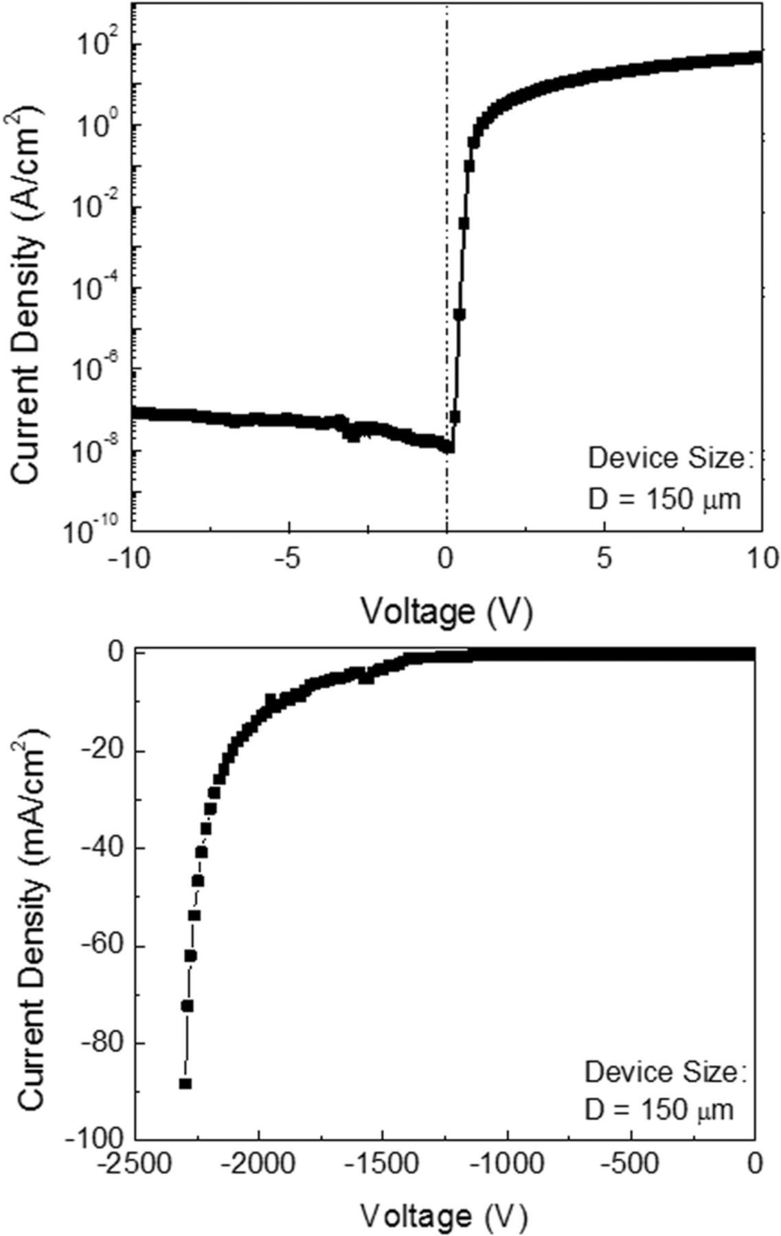
Figure 4. Expanded view of forward (top) and reverse (bottom) J-V characteristics for the 150 μm diameter rectifier that exhibited the largest reverse breakdown voltage of 2300V.
The origin of the leakage current can be determined from the size dependence of current density versus voltage characteristics.42–44 In materials with relatively high surface recombination velocities, surface processes may dominate over bulk carrier transport. Figure 5 shows that the reverse leakage at a fixed bias of 50V scales more with area than perimeter, indicating that bulk processes still dominate in our rectifiers.

Figure 5. Reverse leakage current at a bias of 50V, as a function of either rectifier area (top) or perimeter (bottom).
Figure 6 (top) shows the temperature dependence of forward J-V characteristics from 25–125°C for the 150μm rectifiers. The ideality factor (n) at each temperature was estimated by fitting the linear region of the J–V curve to the thermionic emission (TE) model.13–16 The effective barrier height at zero bias was found to be 1.05 eV from this J-V-T data by linear fitting to the Richardson's plot shown at the bottom of Figure 6. This also produced a Richardson's constant of 43.35 A.cm−2K−2, which is generally in line with previous reports.16,45

Figure 6. Forward current density as a function of temperature (top) and the Arrhenius plot of JO/T2 to obtain the Richardson's constant bottom.
Figure 7 shows the variation of barrier height and ideality factor on temperature for the range 25–125°C for the 150μm rectifiers. The barrier height decreases with temperature, as reported by a number of groups36,39 and is an indication that there may be several transport mechanisms present at elevated temperature. The temperature dependence of I-V provides information regarding both transport mechanism and barrier height, but both are dependent on the particular transport model. To obtain a more direct determination of barrier height, internal photoemission is attractive. Previous reports40 have shown good correlation between both methods for Ga2O3 of the same basic type as used here.

Figure 7. Temperature dependence of Ni Schottky barrier height and diode ideality factor as a function of temperature.
Figure 8 shows the reverse recovery characteristics when switching from +2 V to −2 V, with a recovery time of order 22 ns. In this measurement a 50Ω resistor was used in series with the rectifier. The recovery time is comparable to previous reports with much smaller rectifier dimensions.14,15

Figure 8. Reverse recovery measurement when switching from +2V to –2 V.
Conclusions
In summary, β-Ga2O3 Schottky rectifiers with record reverse breakdown voltages were fabricated on 20 μm thick, very lightly doped (∼2 × 1015 cm−3) drift regions. The breakdown voltage generally decreased with rectifier area and the reverse current was dominated by bulk transport. Future efforts should focus on minimizing Ron while continuing to increase breakdown voltage and finding the appropriate niche for high-speed switches made from this material. The results show that β-Ga2O3 Schottky rectifiers are promising candidates for high power switching devices at voltages above those accessible to GaN and SiC.
Acknowledgments
The project at UF was sponsored by the Department of the Defense, Defense Threat Reduction Agency, HDTRA1-17-1-011, monitored by Jacob Calkins. The content of the information does not necessarily reflect the position or the policy of the federal government, and no official endorsement should be inferred. Research at NRL was supported by the Office of Naval Research, partially under Award Number N00014-15-1-2392. Part of the work at Tamura was supported by "The research and development project for innovation technique of energy conservation" of the New Energy and Industrial Technology Development Organization (NEDO), Japan. Research at Novel Crystal Technology is partially supported by ONR Global (grant # N62909-16-1-2217). We also thank Dr. Kohei Sasaki from Tamura Corporation for fruitful discussions.
ORCID
F. Ren 0000-0001-9234-019X
S. J. Pearton 0000-0001-6498-1256