Abstract
Bound to complex perovskite systems, ferroelectric random access memory (FRAM) suffers from limited CMOS-compatibility and faces severe scaling issues in today's and future technology nodes. Nevertheless, compared to its current-driven non-volatile memory contenders, the field-driven FRAM excels in terms of low voltage operation and power consumption and therewith has managed to claim embedded as well as stand-alone niche markets. However, in order to overcome this restricted field of application, a material innovation is needed. With the ability to engineer ferroelectricity in HfO2, a high-k dielectric well established in memory and logic devices, a new material choice for improved manufacturability and scalability of future 1T and 1T-1C ferroelectric memories has emerged. This paper reviews the recent progress in this emerging field and critically assesses its current and future potential. Suitable memory concepts as well as new applications will be proposed accordingly. Moreover, an empirical description of the ferroelectric stabilization in HfO2 will be given, from which additional dopants as well as alternative stabilization mechanism for this phenomenon can be derived.
Export citation and abstract BibTeX RIS

This is an open access article distributed under the terms of the Creative Commons Attribution Non-Commercial No Derivatives 4.0 License (CC BY-NC-ND, http://creativecommons.org/licenses/by-nc-nd/4.0/), which permits non-commercial reuse, distribution, and reproduction in any medium, provided the original work is not changed in any way and is properly cited. For permission for commercial reuse, please email: oa@electrochem.org.
The recent success of smartphones and tablet computers has accelerated the R&D of fast and energy efficient non-volatile semiconductor memories, capable of replacing the conventional SRAM-DRAM-Flash memory hierarchy. These so called emerging memories usually leverage on the fact that certain materials possess the capacity for remembering their electric, magnetic or caloric history. For the extensively investigated ferroelectrics this ability to memorize manifests in atomic dipoles switchable in an external electric field. This unique property renders them the perfect electric switch for semiconductor memories. Consequently, only a few years after the realization of a working transistor the first ferroelectric memory concepts were proposed.1
However, more than 60 years and several iterations later it is now clear that the success or failure of FRAM is mainly determined by the proper choice and engineering of the ferroelectric material. Perovskite ferroelectrics and related electrode systems underwent an extensive optimization process to meet the requirements of CMOS integration and are now considered the front up solution in FRAM manufacturing. Nevertheless, those perovskite systems require complex integration schemes and pose scaling limitations on 1T and 1T-1C memory cells that until now remain unsolved. This creates an unbalance between memory performance on the one side and manufacturing and R&D costs on the other side. This dilemma has ever since restricted FRAM to niche markets.
With the recent demonstration of ferroelectricity in HfO2-based systems (FE-HfO2) a CMOS-compatible, highly scalable and manufacturable contender has emerged, that significantly expands the material choice for 1T and 1T-1C ferroelectric memory solutions (Reference 2 and references therein) as well as nanoscale ferroelectric devices.
In this paper we will review and expand the current understanding of ferroelectricity in HfO2, as well as discuss future prospects of ferroelectric HfO2-based devices with respect to scaling, reliability and manufacturability. Opportunities and drawbacks of this disruptive development in ferroelectric material science will be critically examined.
Ferroelectric Hafnium Oxide
Basics
In recent years extensive research has been conducted on HfO2 and ZrO2 based thin films and related deposition methodologies. The renewed interest in thin films of these thoroughly investigated ceramic systems was mainly driven by scaling considerations in microelectronics engineering and the industry's striving to find a suitable "high-k" replacement for integrated gate and capacitor dielectrics. As part of this development and in accordance with earlier investigations of bulk ceramics and powders several methodologies were identified to influence the polymorphism of crystalline phases in HfO2 and ZrO2 based systems. The stabilization of the desired higher-k tetragonal or cubic phase against the monoclinic phase was found to depend on doping (Table I and references therein), thermal treatments,3–5 deposition methodology/chemistry and growth temperature,6,7 surface energy effects and strain given by grain size and film thickness,4,5 as well as on the mechanical encapsulation provided by the electrodes.8
Table I. Correlation of phase stabilizing dopants known from literature and the appearance of ferroelectricity in HfO2.
| Dopant < 20 mol% | Known Phase Stabilizer in HfO2 | Ferroelectric properties2 |
|---|---|---|
| Al+3 | Yes (Ref. 11, 12) | confirmed |
| Ca+2 | Yes (Ref. 13) | expected |
| Ce+4 | Yes (Ref. 14, 15) | expected |
| Dy+3 | Yes (Ref. 16, 17) | expected |
| Er+3 | Yes (Ref. 16) | expected |
| Gd+3 | Yes (Ref. 16, 12) | confirmed |
| Ge+4 | Yes (Ref. 18, 15, 12) | expected |
| La+3 | Yes (Ref. 4) | confirmed |
| Sc+3 | Yes (Ref. 17, 12) | expected |
| Si+4 | Yes (Ref. 4, 15, 12) | confirmed |
| Sr+2 | Similar to Ca+2 | confirmed |
| Sn+4 | Yes (Ref. 15, 12) | expected |
| Y+3 | Yes (Ref. 12, 19) | confirmed |
However, detailed structural as well as electrical investigations of Si-doped HfO2 thin films conducted by Böscke et al.9 in 2011 revealed deviations from the commonly assumed polymorphism (monoclinic-tetragonal-cubic). This led to the rediscovery of an intermediate orthorhombic phase that was first and until then solemnly identified in Mg-doped, partially stabilized ZrO2 by Kisi et al.10 in 1989. The ferroelectric nature of this non-centrosymmetric phase in HfO2 thin films is confirmed by characteristic features in its hysteretic P-V, C-V and macroscopic (double beam laser interferometry, DBLI) as well as microscopic (piezoresponse force microscopy, PFM) electromechanical response.9,2
The intrinsic nature of ferroelectricity in HfO2 and therewith the correlation to its relative phase stability is supported by the systematic shown in Table I. Besides Si other known phase stabilizers in HfO2, such as Y or Al, were later found to provoke ferroelectricity in a similar manner. During those investigations the precise stoichiometry control provided by atomic layer deposition proved highly valuable to detect the electrical and structural impact of small dopant quantities in HfO2. This sequential and self-limiting growth technique allows for the insertion of sub-monolayer quantities of the dopant material during thin film growth by simply adjusting the cycling ratio of the host and the dopant precursor pulsing scheme. The linear incorporation of the various dopant species with variable cycling ration was detected by X-ray photoelectron spectroscopy and quantified by the standard free Rutherford backscattering spectroscopy.
Suitable, but with respect to ferroelectric properties until now untested dopants are additionally suggested in Table I. Based on the corresponding literature given in the table, these dopants are also known to influence phase stability in HfO2 and therewith provide the basic requirement of destabilizing the monoclinic phase at room temperature. Due to this commonality with the already investigated systems, the appearance of an intermediate orthorhombic phase appears possible.
However, following this line of argumentation and considering the multiple parameters influencing phase stability in HfO2 stated above, it is further suggested that ferroelectricity in this system is not restricted to doping alone. The recent demonstration of ferroelectricity in the HfO2-ZrO2 solid solution can be viewed as an example where surface energy differences between crystalline phases of HfO2 and ZrO2 can be utilized to achieve a similar kind of transition.20 Consequently, using some of the additional parameters provided above, details of which will be published elsewhere, the stabilization of a ferroelectric phase in pure HfO2 has proven possible (Fig. 1).
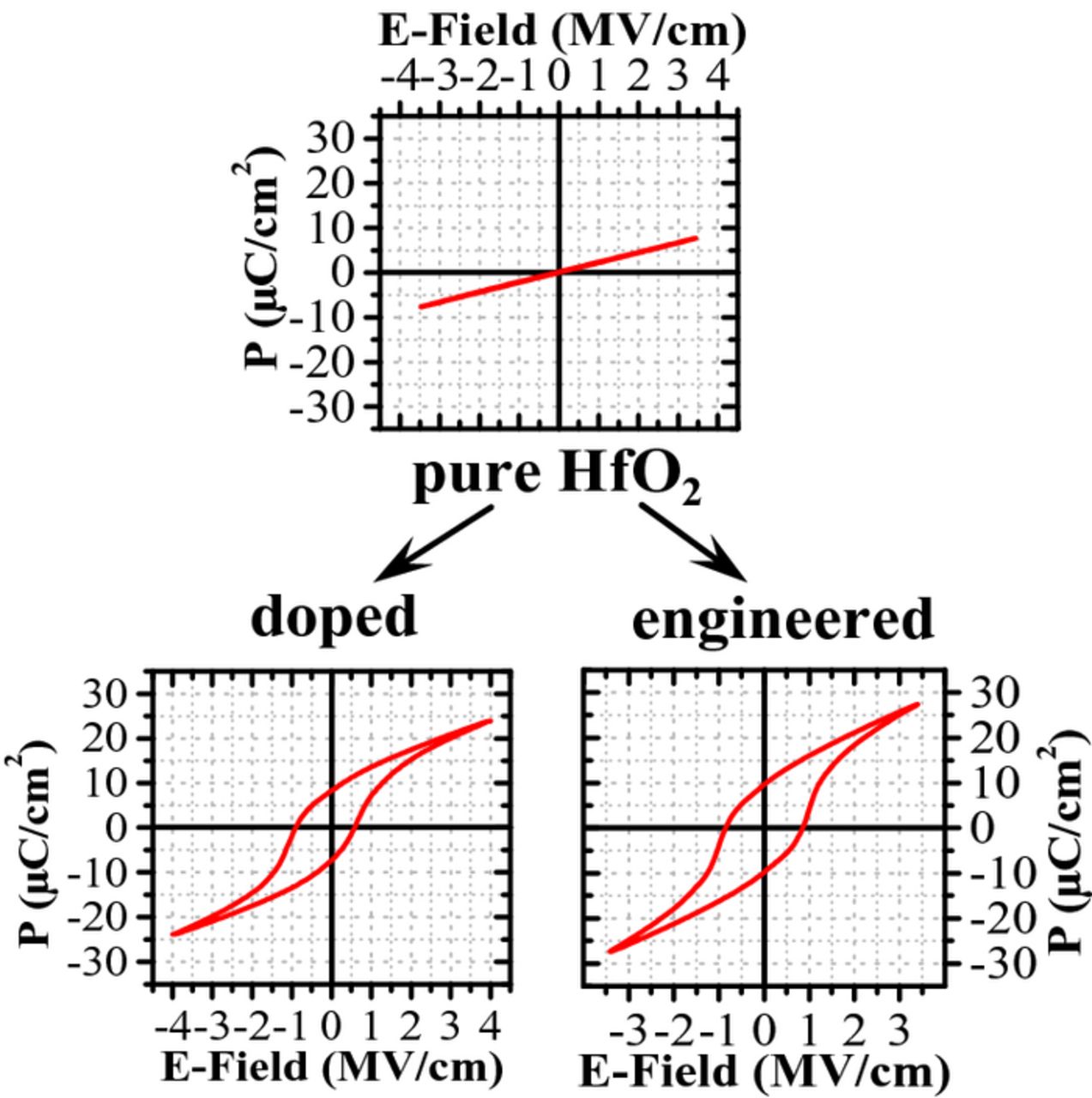
Figure 1. Paraelectric P-E-characteristics of pure HfO2 transitioning to a ferroelectric P-E-hysteresis in doped (e.g. 3.6 mol% Si in Si:HfO2) or engineered (e.g. grain size, encapsulation) HfO2.
Supportive of this argumentation are earlier21 as well as more recent2,22 ab initio simulations that found that the relative stability of this orthorhombic phase in HfO2 and ZrO2 suggested by Kisi et al. lies within a narrow energy range of the commonly assumed polymorphism. Moreover, due to this small energy difference between polar and non-polar phases in HfO2 and ZrO2 it is assumed that the experimentally observed double hysteresis loop in samples close to the ferroelectric stability region can be attributed to a field driven, ferroelectric phase transition.20,23
Material properties and scalability
The coercive field strength Ec and remanent polarization Pr are the most important parameters to describe the hysteretic behavior and functionality of a ferroelectric material. In practice, however, additional parameters such as CMOS-compatibility, scalability, available thin film technologies and thermal budget requirement/tolerance are equally important and decisive upon the applicability of a ferroelectric to microelectronic engineering. In this context Table II summarizes key parameters of FE-HfO2 and compares them to the common perovskite based ferroelectrics. Due to its stable ferroelectric properties at film thicknesses in the single digit nanometer range and straightforward implementation into a standard CMOS-environment, FE-HfO2 emerges as an ideal material choice for high density integration of ferroelectric devices.
Table II. Comparison of FE-HfO2 to the most common perovskite ferroelectrics.
| SrBi2Ta2O9 (SBT) | Pb(ZrxTi1-x)O3 (PZT) | FE-HfO2 | |
|---|---|---|---|
| Film thickness | >25 nm | >70 nm | 5–30 nm |
| Annealing temp. | >750°C | >600°C | 450°C–1000°C |
| Pr | <10 μC/cm2 | 20–40 μC/cm2 | 1–40 μC/cm2 |
| Ec | 10–100 kV/cm | ∼50 kV/cm | 1–2 MV/cm |
| EBD | ∼2 MV/cm | 0.5–2 MV/cm | 4–8 MV/cm |
| Ec/EBD* 100 | 0.5–5% | 2.5–10% | 12.5–50% |
| Dielectric constant | 150–250 | ∼1300 | ∼30 |
| ALD capability | limited | limited | mature |
| CMOS compatibility | Bi and O2 diffusion | Pb and O2 diffusion | stable |
| BEOL compatibility | H2 damage | H2 damage | stable |
| References | 24–27 | 28, 27, 25 | 29, 9, 2, 20, 30–33 |
Special attention needs to be paid to the extraordinary high coercive field strength of FE-HfO2. This rather unique property of FE-HfO2 is crucial to the major scaling advantages as well as reliability disadvantages of this new ferroelectric material.
The scaling advantage is twofold. The high Ec of FE-HfO2 allows for a gate length scaling of the ferroelectric field effect transistor (FeFET, see next section) while at the same time providing a high resilience toward internal depolarization of the ferroelectric. This internal depolarization is intrinsic to the metal-ferroelectric-insulator field effect transistor (MFIS-FET), but can also occur in metal-ferroelectric-metal (MFM) capacitors due to the so called "dead layer effect" at the electrode interfaces.34 Considering such a paraelectric interfacial or depletion layer of a non-ideal electrode with a thickness dPE and a permittivity ɛPE the resulting depolarization field Edep is given by:
![Equation ([1])](https://content.cld.iop.org/journals/2162-8777/4/5/N30/revision1/jss_4_5_N30eqn1.jpg)
Assuming an invariable dead layer it can be deduced that with decreasing ferroelectric thickness dFE the depolarization field increases. For simplicity and in favor of an underestimation of the depolarization field in the high permittivity perovskites, we assume  . Based on Eq. 1 and as illustrated in Fig. 2 it can be readily understood that a high coercive field strength prevents depolarization even at decreased layer thickness and therewith provides stable ferroelectric properties. Consequently, Fig. 3 provides experimental proof that FE-HfO2 preserves its ferroelectric properties down to a film thickness of 5 nm. It should be noted that this thickness does not yet represent a fundamental limit of ferroelectricity in hafnium oxide. At this point in time the issues that arise when decreasing thickness further are rather technological in nature. These are mainly leakage current and reliability related problems due to a change in the conduction mechanism, an increasing crystallization temperature and an increasing impact of electrode roughness in the MFM configuration. Alternative methods such as PFM might be required to access the fundamental thickness scaling limit of ferroelectricity in HfO2.
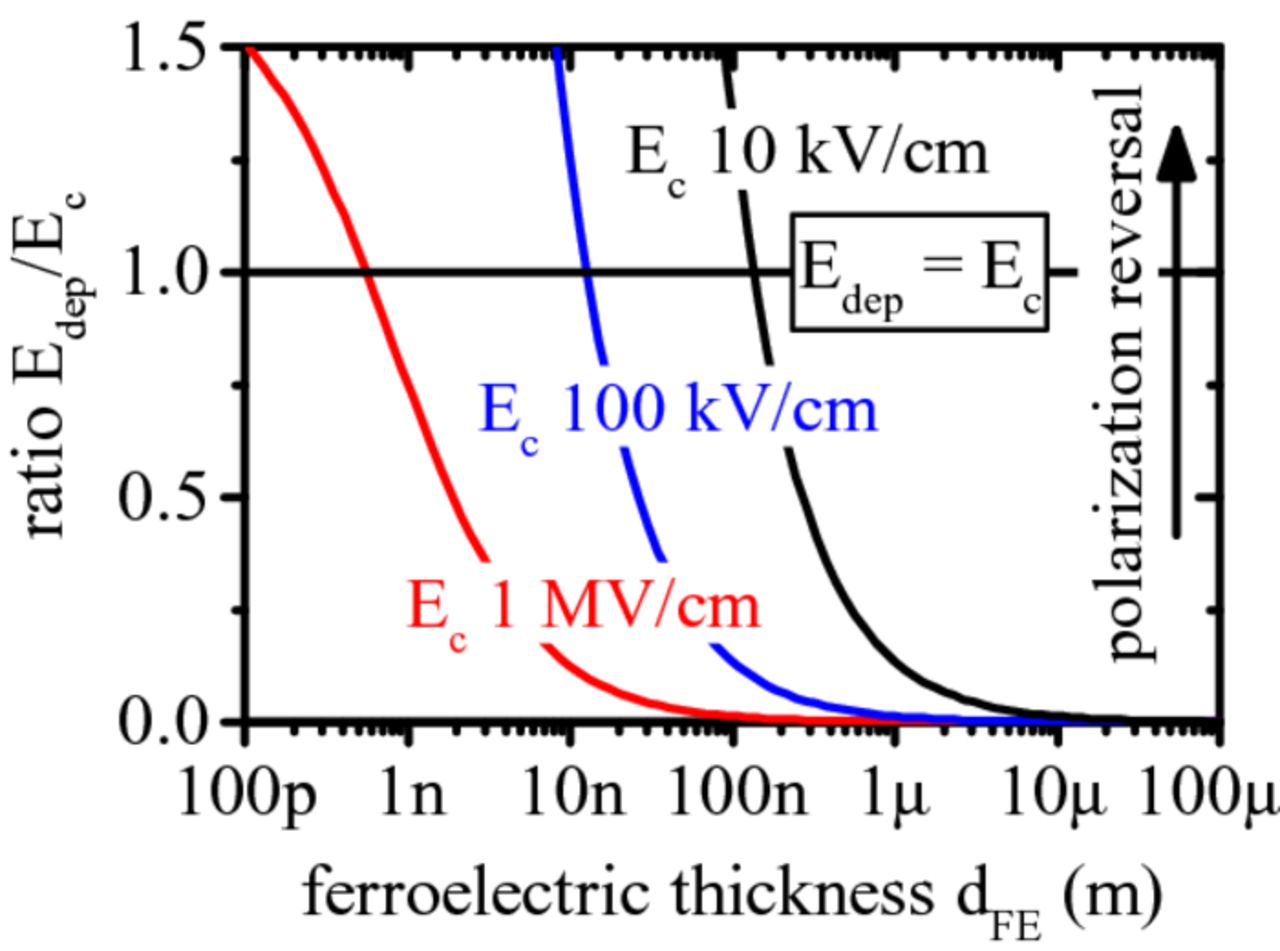
Figure 2. Calculated impact of ferroelectric thickness dFE on the depolarization relevant ratio of Edep/Ec for three different Ec in an MFM capacitor (Eq. 1). Assuming a dead layer of 4 Å and simplification to  .
.
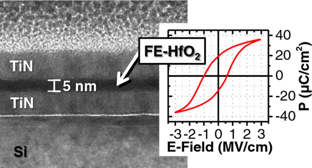
Figure 3. TEM micrograph of an FE-HfO2 based MFM capacitor scaled to a ferroelectric film thickness of 5 nm and related P-E-hysteresis. The HfO2-ZrO2 solid solution with a ratio of 1:1 was chosen as an FE material and sandwiched between two TiN electrodes.
However, in terms of reliability and low voltage operation the high coercive field strength of FE-HfO2 needs to be viewed rather critical. Table II introduces the ratio between the coercive field strength and the field necessary for a hard dielectric breakdown (HBD) as a new figure of merit. It can be seen that compared to its perovskite contenders the dielectric breakdown strength and the operating window for ferroelectric polarization hysteresis in FE-HfO2 lies within the same order of magnitude. Consequently, it has been shown that an abrupt HBD rather than slower, defect mediated mechanism observed in classical ferroelectric fatigue are the major reliability concern in FE-HfO2, whose MFM endurance is currently limited to about 109 switching cycles.30,31 As a consequence, strength and weakness provided by the high coercive field strength in FE-HfO2 needs to be considered when designing appropriate devices and applications.
Memory Applications
From FRAM to NV-DRAM
Classical FRAM is usually realized as a 1T-1C or 2T-2C memory cell. Like in the volatile DRAM the memory state of this cell is defined by the (polarization-) charge stored in a capacitor element, which can be accessed via a cell transistor (Fig. 4a–4b). However, when using a ferroelectric material instead of a linear capacitor dielectric this memory state becomes nonvolatile. To realize this bipolar ferroelectric switching, an additional plate line is added to the common cross point setup of word and bit lines known from DRAM.
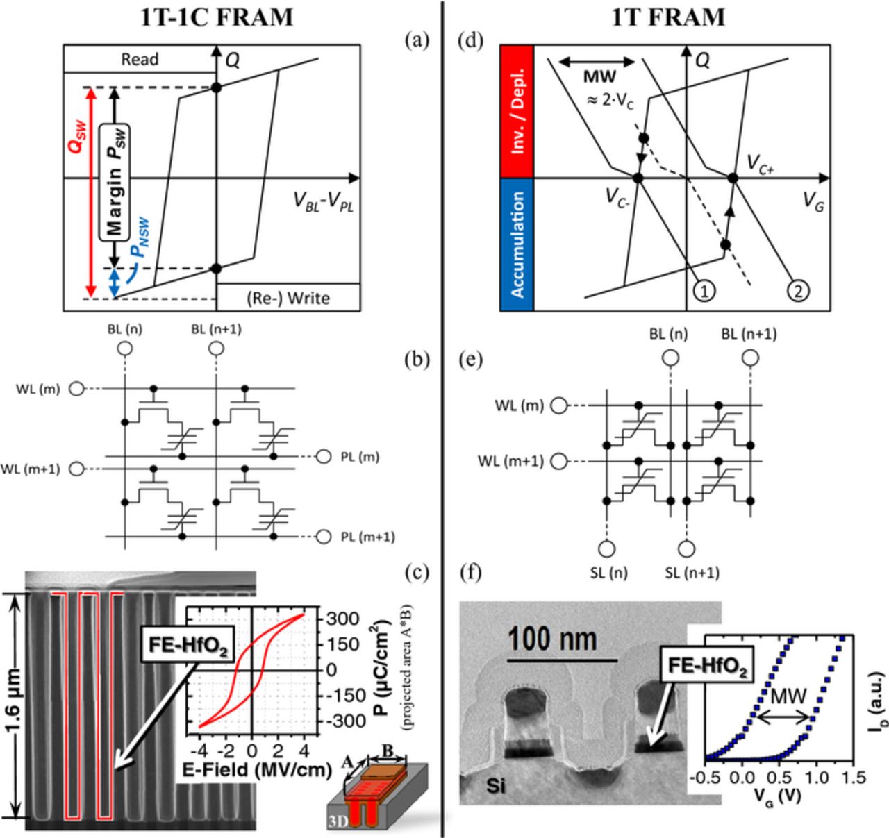
Figure 4. Comparison of the two major flavors of FRAM. 1T-1C: (a) Working principle illustrating the sensing margin / switched polarization Psw derived from switched charge Qsw and non-switched polarization Pnsw in the P-E-hysteresis. (b) DRAM-like architecture of FRAM adding a plateline to word- and bitline for bipolar ferroelectric switching. (c) TEM-micrograph and related P-E-hysteresis of a FE-HfO2 based deep trench capacitor array proving the concept of 3D-integration capability. To illustrate the advantage of this area enhancement, the polarization density is calculated with respect to the lateral footprint of a comparable planar capacitor.30,2 1T: (d) Illustration of the working principle by a graphical representation of the charge neutrality condition in a MFIS stack. Position 1 and 2 of the insulator-semiconductor loadline represents the transition from the ON-state to the OFF-state of the FeFET or vice versa. Accordingly, the gate voltage difference to turn on/off the FeFET can be approximated by 2 · VC = 2 · Ec · dFE, i.e. the memory window MW. (e) Disturb resilient AND architecture of the FeFET. (f) TEM-micrograph and related ID-VG-hysteresis of a FE-HfO2 based 28 nm high-k metal gate transistors proving the concept of advanced 1T FRAM scalability.32
Besides this minor increase in complexity, FRAM and DRAM are quite alike, using comparable sensing schemes and consequently facing similar scaling challenges in terms of decreasing lateral area and therewith decreasing values of absolute (polarization-) charge per bit. In the case of high density standalone and most recent in the case of embedded DRAM (e.g. BEOL trench capacitors35), this issue has been counteracted by extending the capacitor area into the third dimension. For FRAM to follow a similar pathway has proven rather challenging.36 This is mainly due to the high complexity and limited thickness scalability of perovskite ferroelectrics (compare Table II). Considering FE-HfO2 as a material choice for FRAM, these limitations can be overcome. Using a similar material combination like in the metal-insulator-metal (MIM) capacitor of advanced DRAM, an MFM capacitor can be implemented into high aspect ratio structures with minimal planar Pr penalty30,2 (Fig. 4c). Additionally, the stability of the polarization state according to FRAM retention requirements for 10-year data storage has been proven at elevated temperature.31
Besides these promising results, it should be noted that due to the destructive read out in the 1T-1C FRAM concept not only the write, but also the read operation is limited by the cycling endurance of the ferroelectric material. Taking into account the comparably low endurance of FE-HfO2 addressed in the previous section, the potential field of application appears severely limited. Due to the fundamental issue of the coercive field being close to HBD, considerable improvement of switching endurance and therewith read endurance beyond 1010 remains questionable.
However, considering the high endurance and low retention requirements of a NVM during power on and vice-versa for power off, a solution to this problem may lie in a hybrid mode, including volatile and nonvolatile memory operation. Due to the many similarities of HfO2- and ZrO2-based DRAM and FE-HfO2 based FRAM, a manufacturable NV-DRAM solution can be realized. Unlike in conventional NV-DRAM the need to include a separate NVM-element for power off data storage into the DRAM cell becomes obsolete. As depicted in the simplified schematic in Fig. 5, the switch between volatile DRAM and nonvolatile FRAM operation mode is defined by the operating voltage alone. As summarized in Table III the volatile mode, defined by heavy memory usage, provides unlimited read endurance, whereas the nonvolatile mode provides sufficient retention for scheduled/unscheduled power off/loss.
Table III. Performance of FE-HfO2 based 1T-1C and 1T concepts for different operating schemes.
| Cell concept | Operating mode | Read endurance | Write endurance | Retention |
|---|---|---|---|---|
| 1T-1C | FRAM | ∼109 | ∼109 | >10 y |
| DRAM | unlimited | unlimited | <1 s | |
| 1T | Mode 1 (low VG) | unlimited | 1014 | <103 s |
| Mode 2 (high VG) | unlimited | 104–105 | >10 y |
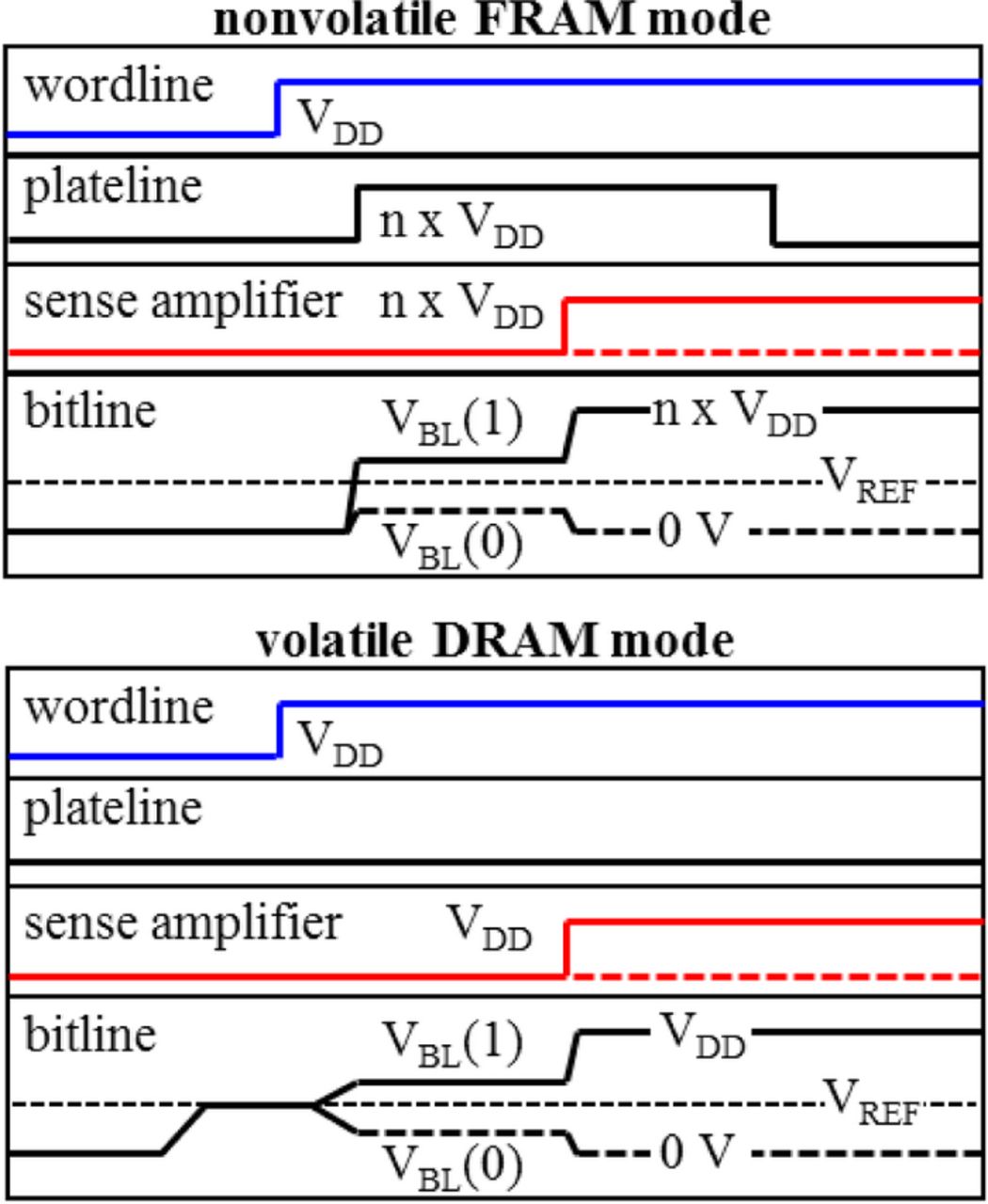
Figure 5. Simplified sensing and operating scheme of a FE-HfO2 based dual mode 1T-1C FRAM. The nonvolatile FRAM mode is provided by polarization reversal activated at boosted VDD, whereas the volatile mode follows standard DRAM operation.
The 1T solution
Compared to the capacitor-based FRAM the ferroelectric field effect transistor provides a smaller cell size and non-destructive read operation. Despite these clear advantages the commercialization of this technology is held back by scaling and CMOS-compatibility issues of the most common MFIS-FET approach. Due to the instability and contamination risk of perovskites in direct contact with silicon, large paraelectric buffer layers have to implemented, which, according to Eq. 1, significantly enhance the internal depolarization and reduce retention time.
Moreover, to achieve a sufficiently large memory window (ΔVt) of the FeFET a large dFE and/or Ec is required (MW ≈ 2 · EC · dFE, Fig. 4d). This leads to the dilemma that when using perovskite ferroelectrics, a relatively large physical height of the gate stack has to be implemented to compensate for small values of Ec (Table II). This increases processing complexity and hinders lateral scaling.
The large Ec and CMOS-compatibility of FE-HfO2 solves both issues addressed above. The recent demonstration of FE-HfO2 based FeFET at the 28 nm node (Fig. 4f) shows that this approach enables scaling alongside high-k metal gate transistor technology.32 This compatibility of an NVM concept to logic is unique and proves its potential as a high density embedded memory technology.
However, also in the case of the MFIS-FET, the ambivalence of the high Ec has to be considered. According to the band diagram depicted in Fig. 6c a large electric field in the insulator evolves when the FE-HfO2 based FeFET is programmed to a saturated, high retention memory window (mode 1 in the MFIS-FET simulation depicted in Fig. 6a–6b). As a consequence severe charge injection into the gate stack leads to a device degradation after only 104–105 switching cycles.32,2 It has been shown that, at the cost of retention, unsaturated programming conditions in combination with a thicker SiO2 interface can be used to significantly enhance the endurance of the FE-HfO2 based FeFET, reaching up to 1014 switching cycles.37 Denoted as mode 2 in Fig. 6a–6b, this retention loss can be understood as a result of the higher Edep and unsaturated polarization hysteresis loops, generally believed to be more prone to depolarization. Similar like in the case of the capacitor based 1T-1C FRAM this tradeoff between endurance and retention (Table III) requires an application-driven design of the memory concept. Both extremes, reaching from NOR-FLASH replacement to a capacitor-less, low refresh rate DRAM are within reach.
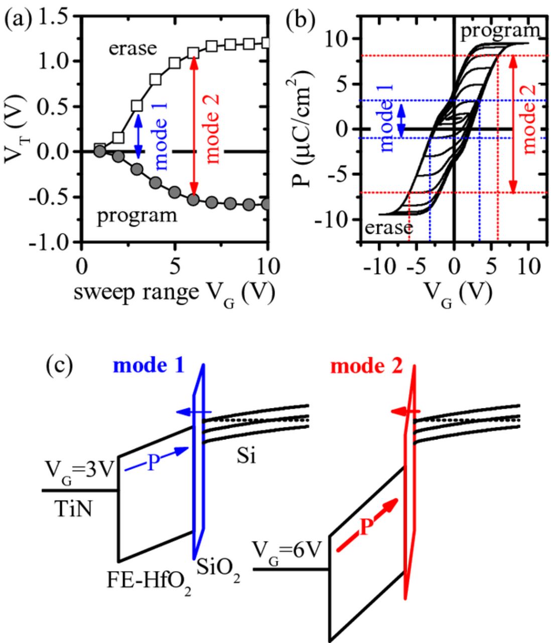
Figure 6. Simulation of a FE-HfO2 based MFIS-FET structure displaying a high endurance mode 1 and a high retention mode 2 (dFE = 10 nm, dPE = 1.2 nm, ɛFE = 32, ɛPE = 3.9, Ec = 1 MV/cm, Pr = 20 μC/cm2). Memory window evolution (a) and polarization (b) as a function of the maximal applied VG. (c) Band bending of the MFIS structure corresponding to the programing conditions of mode 1 and 2.
Finally, considering the most primitive cell array architectures, i.e. AND, NOR and NAND, the most feasible option for FeFET cells is seen in the AND architecture (see Fig 4e). Assuming that each column in a memory array possesses a dedicated sourceline, the so called VDD/3 operational scheme can provide disturb free operation as indicated in previous studies.33 For a common source or NOR architecture, there are no sufficient transistor terminals available that could provide the necessary inhibit signals which are required for avoidance of polarization disturb. Moreover, for a NAND architecture the Vpass and Vprogram disturbs are considered quite critical, however, promising results for SBT-based FeFETs were e.g. presented in Ref. 24.
Beyond Memory
The potential fields of applications for a CMOS-compatible and thickness scalable ferroelectric material clearly reach beyond the scope of classical FRAM. Besides a switchable polarization, the nonlinear capacitance, the electromechanical response, as well as the polarization dependent tunnel barrier of the material offer great potential and may readily be utilized in highly scaled devices.
The increasing miniaturization and circuit complexity of micro-electromechanical systems (MEMS) calls for CMOS-compatible and highly scalable piezoelectric or non-linear materials. Figure 7 compares the mechanical displacement of FE-HfO2 as well as of the field driven transition in antiferroelectric (AFE) HfO2 to the displacement of PZT based thin films. The electromechanical displacement is in the same order of magnitude and proves the feasibility of this new material for MEMS applications. Especially the field driven ferroelectric transition in AFE-HfO2 shows a large displacement, as well as additional potential for energy storage and decoupling capacitor applications utilizing its double loop hysteresis.39
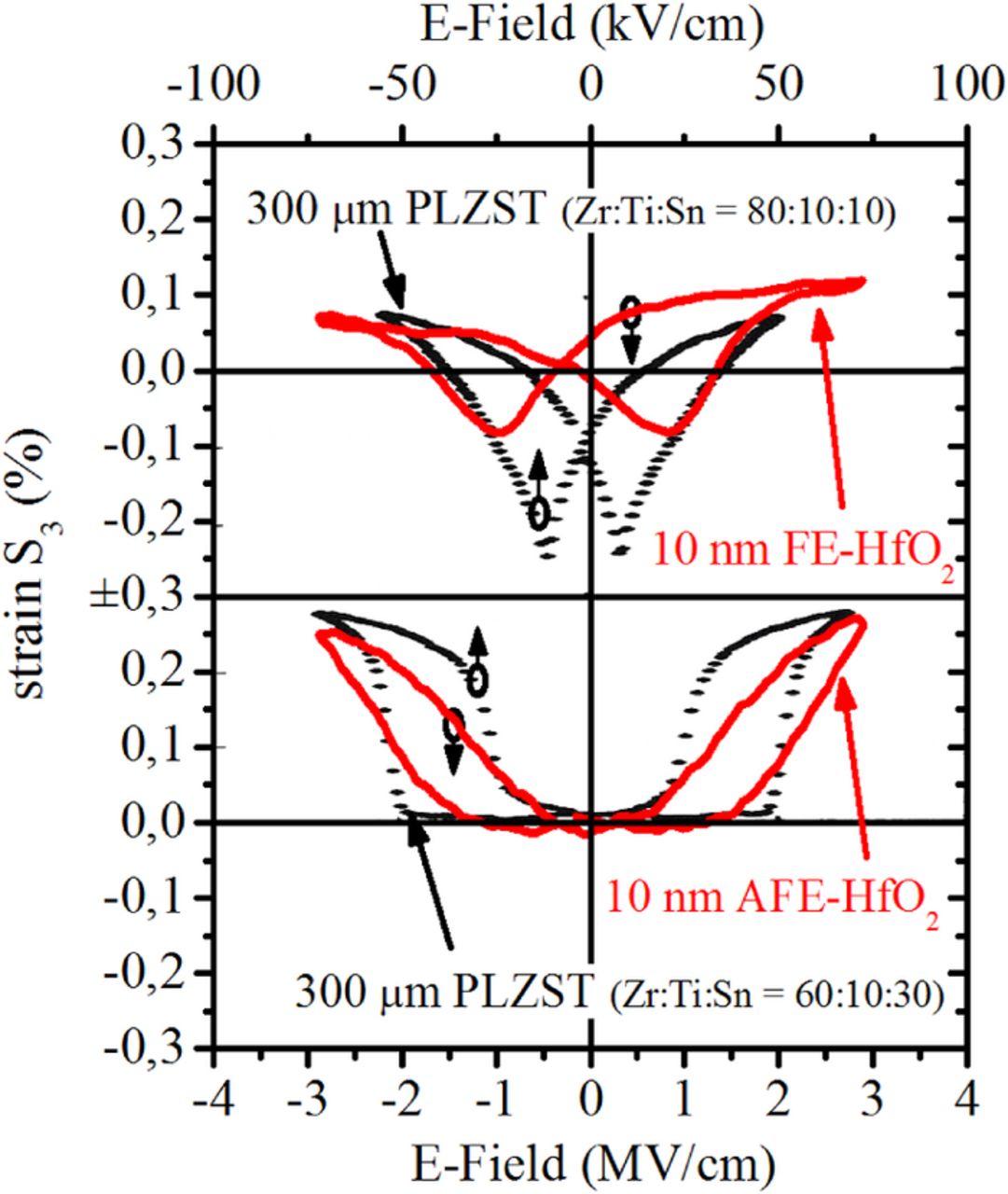
Figure 7. Relative displacement as a function of electric field for 10 nm FE-HfO2 (3.8 mol% Si) and AFE-HfO2 (5.8 mol% Si) measured by DBLI compared to a FE and AFE stoichiometry of 300 μm PLZST (extracted from Ref. 38).
The utilization of the nonlinear dielectric behavior of ferroelectrics to achieve a negative capacitance effect in FeFETs is controversially discussed.40,41 Assuming a working concept of a ferroelectrically induced sub-thermal subthreshold swing, FE-HfO2 as an extensively used material in high-k metal gate transistor technology appears ideally suited. Recent results have demonstrated a clear enhancement of subthreshold slope when using FE-HfO2 as a gate dielectric.42 However, further studies will be needed to identify the true nature of this phenomenon and its effectiveness at real CMOS operating conditions.
Ferroelectric tunnel junctions (FTJs) and other polarization dependent resistive switching phenomena require ferroelectrics that are scalable down to film thicknesses of a few nanometers. Even though FE-HfO2 provides this property, studies following up on this memory concept are still missing. Especially the recent enhancement of the tunneling electroresistivity of FTJs using MIS structures (direct contact with silicon) instead of MIM capacitors underlines the suitability of FE-HfO2 for this kind of concept.43
Conclusions
Ferroelectric HfO2 represents a thickness scalable, CMOS-compatible, processing temperature tolerant and 3D-capable material. The combination of these attributes is unique among ferroelectric materials and opens new pathways for highly dense ferroelectric memories and devices. The high coercive field strength of ferroelectric HfO2 is identified as a crucial parameter to device performance, enabling scaling and currently limiting cycling endurance at the same time. The resulting trade-off between endurance and retention can be tailored to meet the requirements of different memory applications.
Acknowledgments
The work for this paper was supported within the scope of technology development by the EFRE fund of the European Community and by funding from the Free State of Saxony (Project MERLIN / HEIKO / Cool Memory). Further, the authors thank the development teams at GLOBALFOUNDRIES, NaMLab, and Fraunhofer IPMS.